
The most significant differences between the technologies of CMOS and TTL ICs can be seen in their basic inverter/buffer networks, which are used (sometimes in slightly modified form) in virtually every IC within the family range of each type of device. Figures 16 and 17 show the two different basic designs.
The CMOS inverter of Figure 16 consists of a complementary pair of MOSFETs, wired in series, with p-channel MOSFET Q1 at the top and n-channel MOSFET Q2 below, and with both high-impedance gates joined together. The pair can be powered from any supply in the 3–15 V range.
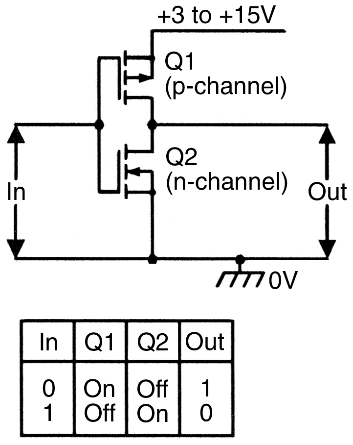
FIGURE 16. Circuit and Truth Table of a basic CMOS inverter.
When the circuit’s input is at logic-0, the basic action is such that Q1 is driven on and Q2 is cut off, and the output is actively pulled high (to logic-1). Note that the output can source (drive) fairly high currents into an external load (via Q1) under this condition, but that the actual inverter stage consumes near-zero current, since Q2 is cut off.
When the circuit’s input is at logic-1, the reverse of this action occurs: Q1 is cut off and Q2 is driven on, and the output is actively pulled low (to logic-0). Note that the output can sink (absorb) fairly high currents from an external load (via Q2) under this condition, but that the actual inverter stage consumes near-zero current, since Q1 is cut off.
Thus, the basic CMOS inverter can be used with any supply in the 3-15 V range, has a very high input impedance, consumes near-zero quiescent current, has an output that switches almost fully between the two supply rails, and can source or sink fairly high output load currents. Typically, a single basic CMOS stage has a propagation delay of about 12-60 nS, depending on supply voltage.
The TTL inverter of Figure 17 is split into three sections, consisting of an emitter-driven input (Q1), a phase-splitter (Q2), and a totem-pole output stage (Q3-D1-Q4). It must be powered from a five-volt supply. When the circuit’s input is pulled down to logic-0, the basic action is such that Q1 is saturated, thus depriving Q2 of base current and causing Q2 and Q4 to cut off, and, at the same time, causing emitter-follower Q3 to turn on via R2 and give an active pull-up action in which the output has (because of various volt-drops) a typical loaded value of about 3.5 V.
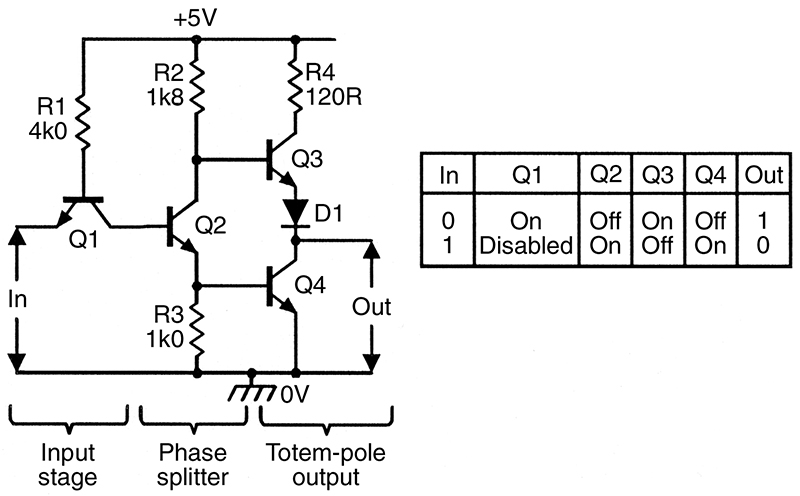
FIGURE 17. Circuit and Truth Table of a basic TTL inverter.
This circuit can source fairly high currents into an external load. Conversely, when the circuit’s input is at logic-1, Q1 is disabled, allowing Q2 to be driven on via R1 and the forward-biased base-collector junction of Q1, thus driving Q4 to saturation and simultaneously cutting off Q3.
Under this condition, Q4 gives an active pull-down action and can sink fairly high currents, while the output takes up a typical loaded value of 400 mV. Note that (ignoring external load currents) the circuit consumes a quiescent current of about 1 mA in the logic-1 output state, and 3 mA in the logic-0 output state.
Thus, the basic TTL inverter can only be used with a five-volt supply, has a very low input impedance, consumes up to 3 mA of quiescent current, has an output that does not switch fully between the two supply rails, and can source or sink fairly high load currents. Typically, a single basic TTL stage has a propagation delay of about 12 nS.
Basic TTL Circuit VariationsThere are five very important variations of the basic Figure 17 TTL inverter circuit. The simplest of these is the so-called “open collector” TTL circuit, which is shown in basic form in Figure 18.
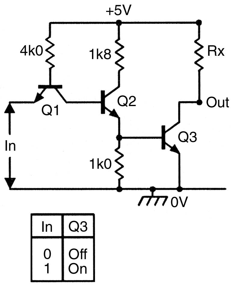
FIGURE 18. TTL inverter with open-collector output.
Here, output transistor Q3 is cut off when the input is at logic-0, and is driven on when the input is at logic-1. Thus, by wiring an external load resistor between the OUT and +5 V pins, the circuit can be used as a passive pull-up voltage inverter that has an output that (when lightly loaded) switches almost fully between zero and the positive supply rail value.
Alternatively, it can be used to drive an external load (such as an LED or relay, etc.) that is connected between OUT and a positive supply rail, in which case the load activates when a logic-1 input is applied.
The second variation is the non-inverting amplifier or buffer. This is made by simply wiring an additional direct-coupled inverter stage between the phase-splitter and output stages of the standard inverter. Figure 19 shows an open collector version of such a circuit, which can be used with an external resistor or load. In this example, Q4 turns on when a logic-0 input is applied.
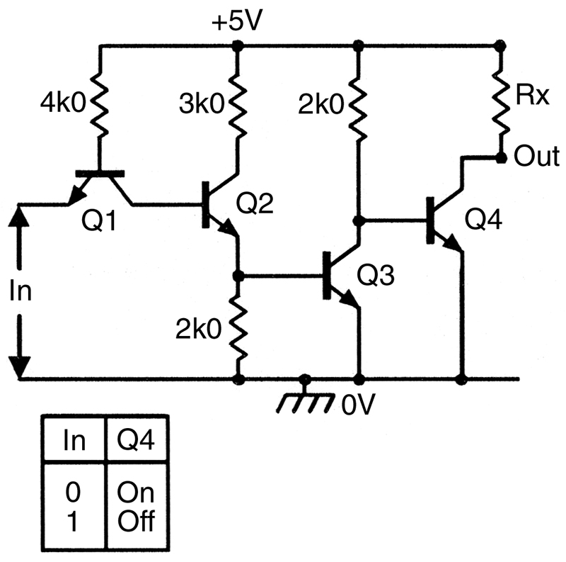
FIGURE 19. TTL non-inverting buffer with open-collector output.
Figure 20 shows a major TTL design variation.
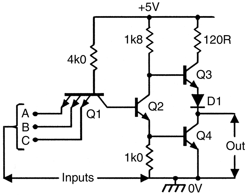
FIGURE 20. TTL three-input NAND gate.
Here, the basic inverter circuit is used with a triple-emitter input transistor, to make a three-input NAND gate in which the output goes low (to logic-0) only when all three inputs are high (in the logic-1 state). Multiple-emitter transistors are widely used within TTL ICs. Some TTL gates use an input transistor with as many as a dozen emitters to make a 12-input gate.
A further variation concerns the use of a “Tri-State” (or “three-state”) type of output that incorporates additional networks plus an external ENABLE control terminal. In one state, the totem-pole output stage operates in its normal logic-0 or logic-1 mode, but in the other state, both totem-pole transistors are disabled (turned off), creating an open-circuit (high impedance) output. This facility is useful in allowing several outputs or inputs to be shorted to a common bus or line, as shown in Figure 21, and to communicate along that line by ENABLING only one output and one input device at a time.
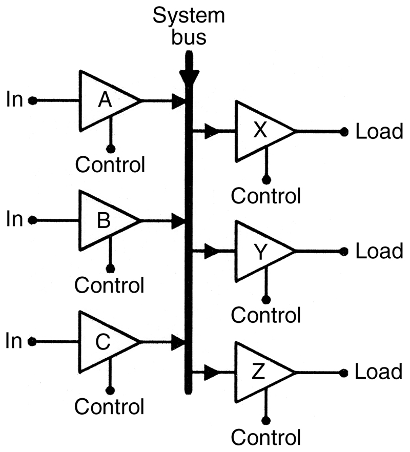
FIGURE 21. Tri-State logic enables several outputs or inputs to be connected to a common bus. Only one output/input must be made active at any given moment.
The final circuit variation is an application one, and concerns the use of an external 2 kΩ pull-up resistor on a totem-pole output stage, as shown in Figure 22.
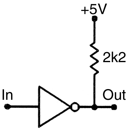
FIGURE 22. An external 2 kW pull-up resistor connected to the output of a totem-pole stage pulls the output to almost +5 V in the logic-1 state.
This resistor pulls the output (when lightly loaded) up to virtually the full +5 V supply value when the output is in the logic-1 state, rather than to only +3.5 V. This is sometimes useful when interfacing the output of a TTL IC to the input of a CMOS IC, for example.
The “74 Series” Digital ICsTTL IC technology first hit the electronics engineering scene in a big way in about 1972, when it arrived in the form of an entire range of digital logic ICs that were exceptionally easy to use. The range was an instant international success, and quickly became the world’s leading IC logic system. Its ICs were produced in both commercial and military grades, and carried prefixes of 74 and 54, respectively; the commercial product range soon became known simply as the “74 series” ICs.
Over the years, the “74 series” ICs have progressively expanded their range of devices and advanced their production technology, so that today the 74 series is as popular and versatile as ever. When first introduced in the early 1970s, the series was based entirely on a simple type of TTL technology, but in later years, new sub-families of TTL were introduced in the series, and then various types of CMOS technology was added to it, so that today’s 74 series incorporates a variety of TTL and CMOS sub-families. Our next installment will take a close look at the sub-families of 74 series ICs, and explain some basic TTL terminology. NV