
Understanding Digital Logic ICs — Part 1
Modern digital logic ICs are widely available in three basic types: TTL devices (typified by the 74LS00 logic family), “slow” CMOS devices (typified by the “4000” logic family), and “fast” CMOS devices (typified by the 74HC00 and 74AC00 logic families). Each of these families has its own particular advantages and disadvantages, and its own special set of usage rules.
This four-part mini-series explains the basic principles and usage rules of each of these three digital logic families, and provides practical usage guidance for the vast range of ICs available in each of these families. This opening article concentrates on digital logic IC basics.
Digital Logic IC BasicsAn IC can be described as a complete electronic circuit or “electronic building block,” integrated into one or more semiconductor slices (or “chips”) and encapsulated in a small, multi-pin package. An IC can be made fully functional by wiring it to a suitable power supply and connecting various pins to appropriate external input, output, and auxiliary networks.
ICs come in both “linear” and “digital” forms. Linear ICs are widely used as pre-amplifiers, power amplifiers, oscillators, and signal processors, etc., and give a basic output that is directly proportional to the magnitude (analog value) of the input signal, which itself may have any value between zero and some prescribed maximum limit.
One of the simplest types of linear IC elements is the unity-gain buffer. If a large sine-wave signal is connected to the input of this circuit, it produces a low-impedance output of almost identical form and amplitude, as shown in Figure 1(a). Digital ICs, on the other hand, are effectively blind to the precise amplitudes of their input signals, and simply recognize them as being in either a low or a high state (usually known as logic-0 and logic-1 states, respectively).
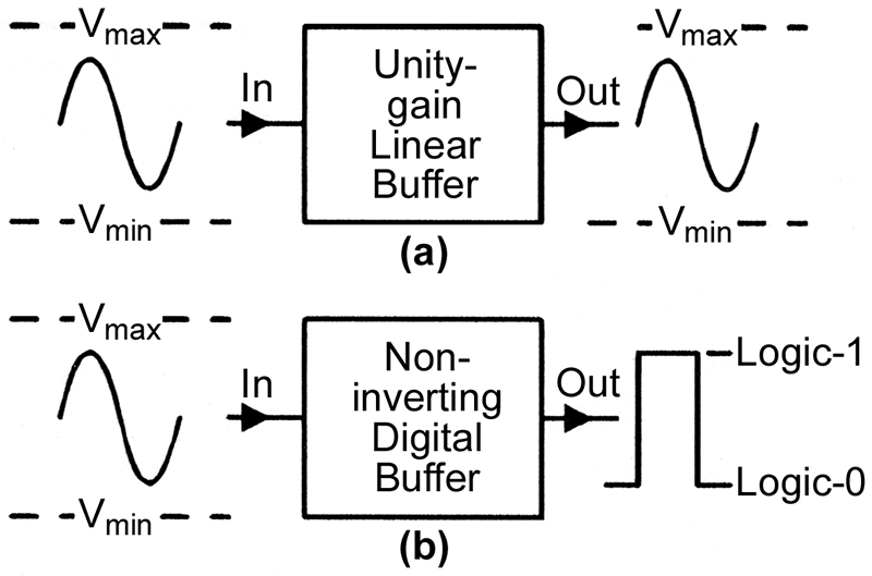
FIGURE 1. When a large input sine wave is fed to the input of a linear buffer (a), it produces a sine-wave output, but when fed to the input of a digital buffer (b), it produces a purely digital output.
Their outputs similarly have only two basic states, either low or high (logic-0 or logic-1). One simple type of digital IC element is the non-inverting buffer. If a large sine-wave signal is connected to the input of this circuit, it produces an output that (ideally) is of purely digital form, as shown in Figure 1(b).
Digital ICs are available in a variety of rather loosely defined categories such as memory ICs, electronic delay-line ICs, and microprocessor support ICs, etc., but the most widely used category is that known as the “logic” type, in which the ICs are designed around fairly simple logic circuits such as digital buffers, inverters, gates, or flip-flop elements. Digital logic circuits come in a variety of basic types and can be built using a variety of discrete or integrated technologies. Figures 2 through 7 show a selection of very simple logic circuits that are designed around discrete components.
Figure 2(a) shows a simple inverting digital buffer (also known as a NOT logic gate), consisting of an unbiased transistor wired in the common-emitter mode, and Figure 2(b) shows the international symbol that is used to represent it. The arrowhead indicates the direction of signal flow, and the small circle on the symbol’s output indicates the inverting action.
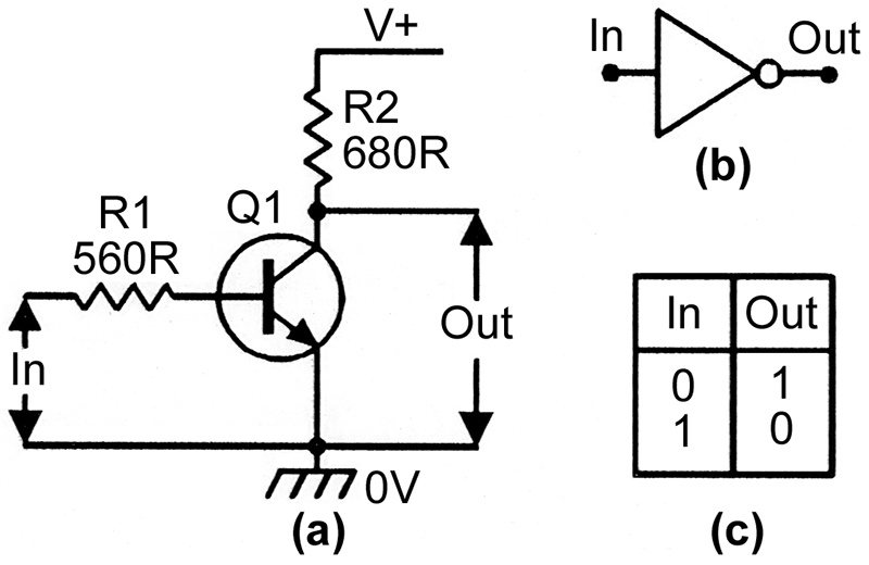
FIGURE 2. Circuit (a), symbol (b), and Truth Table (c) of a simple inverting digital buffer.
The circuit action is such that Q1 is cut off (with its output high) when its input is in the zero state and is driven fully on (with its output pulled low) when its input is high. This information is presented in concise form by the Truth Table of Figure 2(c), which shows that the output is at logic-1 when the input is at logic-0, and vice versa.
Figure 3(a) shows a simple non-inverting digital buffer, consisting of a direct coupled pair of common-emitter (inverter) transistor stages. Figure 3(b) shows the arrow-like international symbol used to represent it. Figure 3(c) shows the Truth Table that describes its action, e.g., the output is at logic-0 when the input is at logic-0, and is at logic-1 when the input is at logic-1.
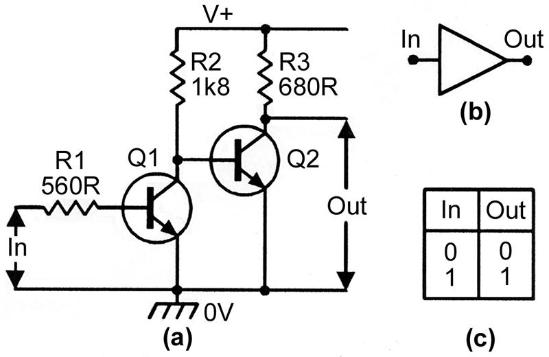
FIGURE 3. Circuit (a), symbol (b), and Truth Table (c) of a non-inverting digital buffer.
In digital electronics, a “gate” is a logic circuit that opens or gives an output (usually defined as a high or logic-1 state) only under a certain set of input conditions. Figure 4(a) shows a simple two-input OR gate, made from two diodes and a resistor, and Figure 4(b) shown the international symbol used to represent it. Figure 4(c) shows its Truth Table (in which the inputs are referred to as A or B). Note that the output goes to logic-1 if A or B goes to logic-1.
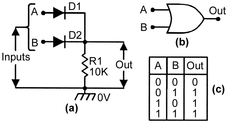
FIGURE 4. Circuit (a), symbol (b), and Truth Table (c) of a simple two-input OR gate.
Figure 5 shows the circuit, symbol, and Truth Table of a two-input NOR (Negated-output OR) gate, in which the output is inverted (as indicated by the output circle) and goes to logic-0 if either input goes high.
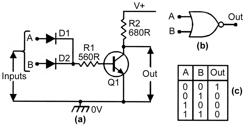
FIGURE 5. Circuit (a), symbol (b), and Truth Table (c) of a two-input NOR gate.
Figure 6(a) shows a simple two-input AND gate, made from two diodes and a resistor, and Figure 6(b) shows its standard international symbol. Figure 6(c) shows the AND gate’s Truth Table, which indicates that the output goes to logic-1 only if inputs A and B are at logic-1.
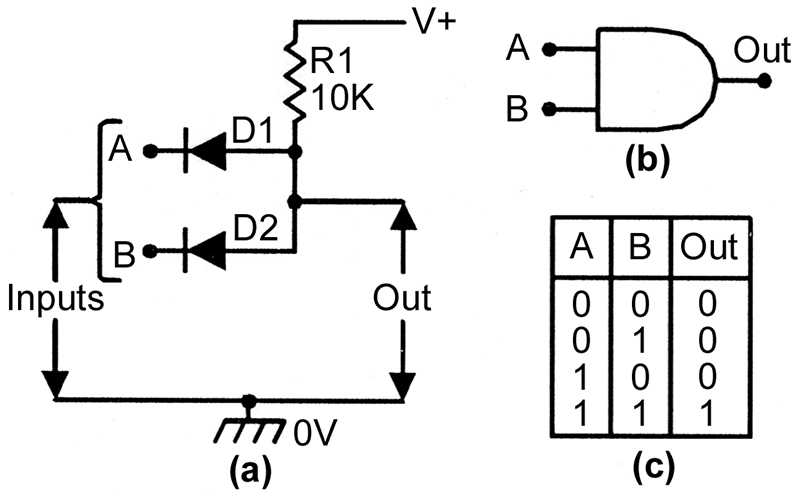
FIGURE 6. Circuit (a), symbol (b), and Truth Table (c) of a simple two-input AND gate.
Finally, Figure 7 shows the circuit, symbol, and Truth Table of a two-input NAND (Negated-output AND) gate, in which the output is inverted (as indicated by the output circle) and goes to logic-0 only if both inputs are at logic-1.
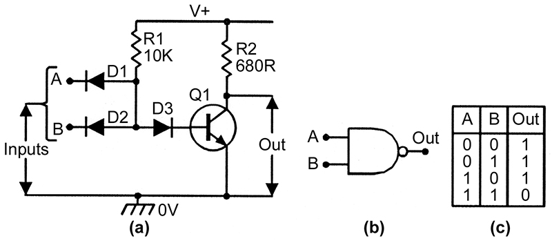
FIGURE 7. Circuit (a), symbol (b), and Truth Table (c) of a two-input NAND gate.
Note that although the four basic types of logic gate circuits described here are each shown with only two input terminals, they can, in fact, be designed or used to accept any desired number of inputs, and can be used to perform a variety of simple logic operations. Many types of digital buffers and gates are readily available in IC form, as are many other digital logic circuits, including flip-flops, latches, shift registers, counters, data selectors, encoders, and decoders.
Practical digital ICs may range from relatively simple logic devices — housing the equivalent of just a few basic gates or buffers — to incredibly complex devices housing the equivalent of tens of thousands of interconnected gates, etc. By convention, the following general terms are used to describe the relative density or complexity of integration:
- SSI (Small Scale Integration) — Complexity level between one and 10 gates.
- MSI (Medium Scale Integration) — Complexity level between 10 and 100 gates.
- LSI (Large Scale Integration) — Complexity level between 100 and 1,000 gates.
- VLSI (Very Large Scale Integration) — Complexity level between 1,000 and 10,000 gates.
- SLSI (Super Large Scale Integration) — Complexity level between 10,000 and 100,000 gates.
Note that most logic ICs of the types described throughout this series of articles have complexity levels ranging from four to 400 gates, and are thus SSI, MSI, or LSI devices. In broad terms, most microprocessor ICs and moderately large memory ICs are VLSI devices, while large dynamic RAM (Random Access Memory) ICs are SLSI devices.
Digital Waveform BasicsDigital logic ICs are invariably used to process digital waveforms. It is thus pertinent at this point to review some basic facts and terms concerning digital waveforms.
Waveforms are available in either square or pulse form. Figure 8 illustrates the basic parameters of a square wave.
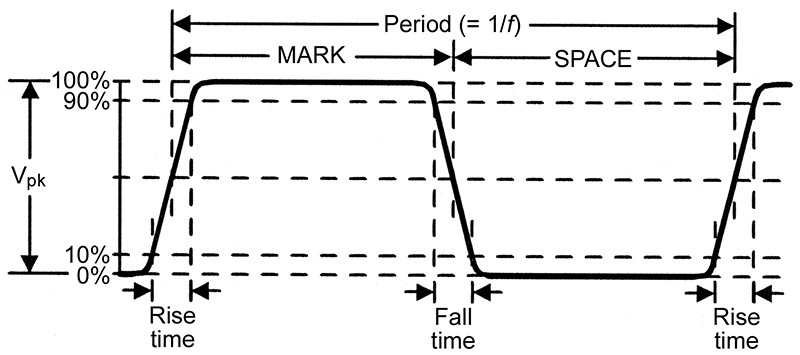
FIGURE 8. Basic parameters of a square wave.
In each cycle, the wave first switches from zero to some peak voltage value (Vpk) for a fixed period, then switches low again for a second fixed period, and so on. The time for the waveform to rise from 10% to 90% of Vpk is known as its rise time, and the time for it to drop from 90% to 10% of Vpk is known as its fall time.
In each square-wave cycle, the high part is known as its mark and the low part as its space. In a symmetrical square wave such as the one in Figure 8, the mark and space periods are equal. Such waveforms are said to have a 1:1 Mark-Space (or M-S) ratio, or a 50% duty cycle (since the mark duration forms 50% of the total cycle period). Square waves are not necessarily symmetrical, but are always free-running or repetitive, i.e., they cycle repeatedly, with consistent mark and space periods.
A pulse waveform is a bit like a square wave. It has both rise and fall times, but only one portion — either its mark or its space period — is specified; the duration of the remaining period is unimportant. Figure 9(a) shows a basic “positive-going” pulse waveform, which has a ‘rising’ or positive-going leading edge, and Figure 9(b) shows a “negative-going” pulse waveform, which has a “falling” or negative-going leading edge. Note that many modern MSI digital ICs, such as counter/dividers and shift registers, can be selected or programmed to trigger on either the rising or the falling edge of an input pulse, as desired by the user.
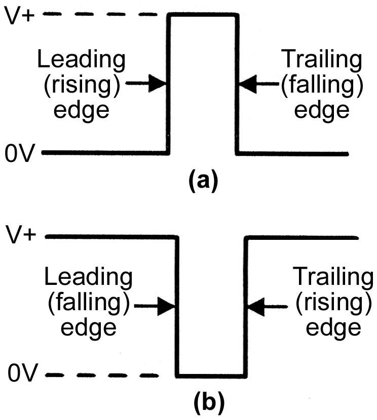
FIGURE 9. Basic forms of (a) “positive-going” and (b) “negative-going” pulses.
If a near-perfect pulse waveform is fed to the input of a real-life amplifier or logic gate, etc., the resulting output waveform will be distorted both in form and time, as shown in Figure 10. Thus, not only will the output waveform’s rise and fall times be increased, but the arrival and termination of the output pulse will be time delayed relative to that of the input pulse.
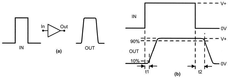
FIGURE 10. A perfect pulse, fed to the input of a practical amplifier or gate, produces an output pulse that is distorted both in form and time. The output pulse’s time delay is called its propagation delay, and (in (b)) = (t1 + t2) / 2.
The mean value of the delays is called the device’s propagation delay. Also, the peaks of the waveform’s rising and falling edges may suffer from various forms of ringing, overshoot, undershoot, etc. The magnitudes of these distortions vary with the quality or structure of the amplifier or gate.
In practice, pulse input waveforms may sometimes be so imperfect that they may need to be “conditioned” before they are suitable for use by modern, fast-acting digital ICs. Specifically, they may have such long rise or fall times that they may have to be sharpened up via a Schmitt trigger before they are suitable for use.
Again, many mechanically-derived pulse waveforms, such as those generated via switches or contact-breakers, may suffer from multiple “contact bounce” problems such as those shown in Figure 11(a). In this case, they will have to be converted to the clean form shown in Figure 11(b) before they can be usefully used.
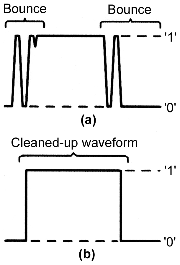
FIGURE 11. Mechanically derived pulse waveforms often suffer from contact bounce (a), and must be cleaned up (b) before use.
Logic FamiliesPractical digital logic circuits and ICs can be built using various technologies. The first successful family of digital logic ICs appeared in the mid 1960s. These used a 3.6 V supply and employed a simple technology that became known as Resistor-Transistor Logic, or RTL. Figure 12 shows the basic circuit for a three-input RTL NOR gate. RTL was rather slow in operation, having a typical propagation delay (the time taken for a single pulse edge or transition to travel from input to output) of 40 nS in a low-power gate, or 12 nS in a medium power gate. RTL is now obsolete.
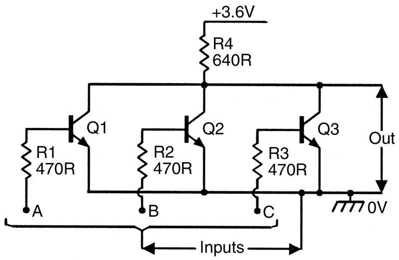
FIGURE 12. IC version of a three-input RTL NOR gate.
Another early type of IC logic technology, developed in the late 1960s, was based on simple developments of the discrete types of logic circuit shown in Figures 2 through 7, and was known as Diode-Transistor Logic, or DTL. Figure 13 shows the basic circuit of a three-input DTL NAND gate. DTL used a dual five-volt power supply, gave a typical propagation delay of 30 nS, and gave an output of less than 0.4 V in the logic-0 state and greater than 3.5 V in the logic-1 state. DTL is now obsolete.
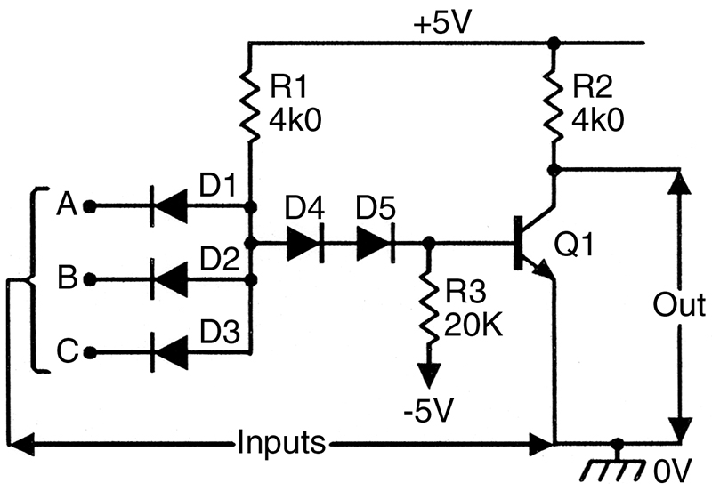
FIGURE 13. IC version of a three-input DTL NAND gate.
Between the late 1960s and mid 1970s, several other promising IC logic technologies appeared. Most of them soon disappeared back into oblivion again. Amongst those that came and either went or receded in importance were HTL (High Threshold Logic), ECL (Emitter Coupled Logic), and PML (P-type MOSFET Logic). The most durable of these technologies was ECL, which is still in production and gives very fast operation, but at the cost of very high current/power consumption.
Figure 14 shows the basic circuit of the ECL digital amplifier — a non-saturating emitter-coupled differential amplifier (Q1 and Q2) with emitter-follower output stages (Q3 and Q4). Because its transistors do not saturate when switched, it gives typical propagation delays of only 4 nS. Note that the circuit’s V+ line is normally grounded and the V- line is powered at -5.2 V.
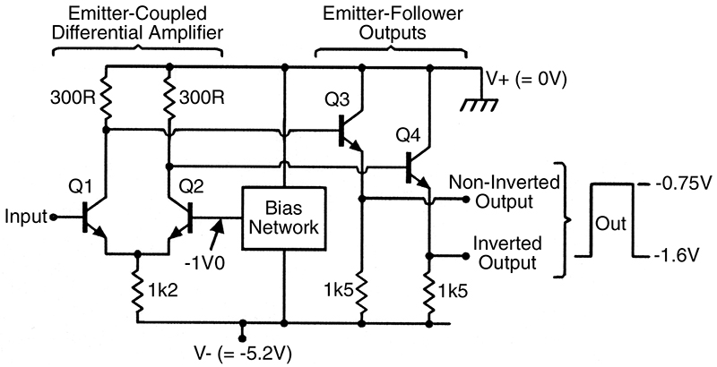
FIGURE 14. Basic ECL (Emitter-Coupled Logic) amplifier circuit.
Under this condition, the circuit provides nominal digital output swings of only 0.85 V, i.e., from a low state of -1.60 V to a high state of -0.75 V. The circuit’s digital input is applied to the base of Q1. A non-inverted output is available on Q3 emitter, and an inverted output is available on Q4 emitter. Modern ECL ICs are used only when ultra high-speed operation is required.
The basic aim of digital IC designers during the late 1960s to early 1970s was to devise a technology that would be simple to use and that achieved a good compromise between high operating speed and low power consumption. The problem here was that conventional transistor-type circuitry, using an output stage of the Figure 2 type (as in RTL and DTL systems), was simply not capable of meeting the last two of these design needs. The essence of this problem — and its ultimate solution — can be understood with the aid of Figure 15.
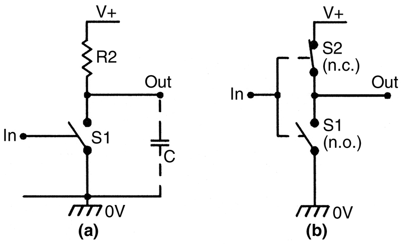
FIGURE 15. (a) Simple digital switch. (b) Basic “totem-pole” digital switch.
Figure 15(a) shows a simplified version of the circuit in Figure 2, with Q1 replaced by a mechanical switch. Remember here that all practical output loads inevitably contain capacitance (typically up to about 30 pF in most digital circuits), so it can be seen that this basic circuit will charge (source current into) a capacitive load fairly slowly via R2 when S1 is open, but will discharge it (sink current from it) rapidly via S1 when S1 is closed; thus, circuits of this type produce digital outputs that tend to have long rise times and short fall times. The only way to reduce the rise time is to reduce the R2 value, and that increases S1’s (Q1’s) current consumption by a proportionate amount.
Note that one good way of describing the deficiency of the Figure 15(a) logic circuit is to say that its output gives an active pull-down action (via S1), but a passive pull-up action (via S2). Obviously, a far better digital output stage could be made by replacing R2 and S1 with a ganged pair of change-over switches, connected as shown in Figure 15(b), so that S2 gives active pull-up action and S1 gives active pull-down action, but so arranged that only one switch can be closed at a time (thus ensuring that the circuit consumes zero quiescent current). Such a circuit — with one electronic switch placed above the other — is called a totem-pole output stage.
Throughout the late 1960s, digital engineers strove to design a cheap and reliable electronic version of the totem-pole output stage, and then — in the early 1970s — they hit the jackpot. Two such technologies hit the commercial market like bombshells and went on to form the basis of today’s two dominant digital IC families. The first of these — based on bipolar transistor technology — is known as TTL (Transistor-Transistor Logic). TTL is the basis of the so-called “74” family of digital ICs that first arrived in 1972.
The second, based on FET technology, is known as CMOS (Complementary MOS-FET logic). CMOS is the basis of the rival “4000-series” (and the similar “4500-series”) digital IC family that first arrived in about 1975. The TTL and CMOS technologies have vastly different characteristics, but both offer specific technical advantages that make them invaluable in particular applications.