Understanding Digital Logic ICs — Part 4 from Rajesh Khatri's blog
Figure 16 expands the above information and shows actual defined threshold voltage and noise margin values, together with typical propagation and power dissipation values for single 00-type two-input NAND gates, for the seven major sub-families of TTL (FAST TTL is regarded here as simply a minor variation of AS TTL).
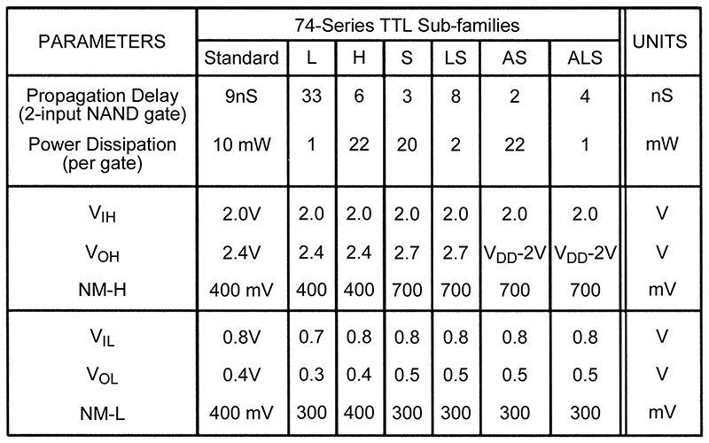
FIGURE 16. Typical propagation delay and power dissipation figures for single 00-type NAND gates within the TTL sub-family ranges, together with sub-family voltage threshold and noise-margin values.
Fan-In and Fan-OutIn TTL circuitry, an element’s input drive requirements are known as its fan-in values, and its output driving capability limits are known as its fan-out values. Figure 17 illustrates the meanings and worst-case values of these items when applied to a Standard TTL element.
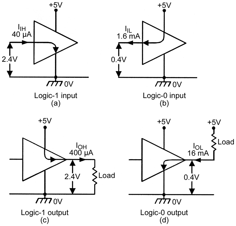
FIGURE 17. Basic input and output parameters of a Standard TTL logic element.
Thus, (a) shows that when the TTL element is driven from a Standard TTL output stage, it draws a worst-case input current (IIH) of 40µA when fed with a 2.4 V logic-1 input, but — as shown in (b) — feeds 1.6 mA (IIL) into the driver when it provides a 0.4 V logic-0 input. Diagram (c) shows that the TTL element’s output can, when in the logic-1 state, provide up to 400µA (IOH) before its output voltage falls below 2.4 V; it is thus capable of feeding up to 10 Standard inputs, and is said to have a logic-1 fan-out (= IOH/IIH) of 10.
Similarly, (d) shows that the output stage can — when in the logic-0 state — absorb up to 16 mA before its output voltage falls below 0.4 V; it is thus capable of driving up to 10 Standard inputs, and is said to have a logic-0 fan-out (= IOL/IIL) of 10. Thus, the element has a worst-case fan-out of 10, and it can be used to directly drive as many as 10 Standard inputs.
Figure 18 presents the above data in tabular form, together with similar data for all other major TTL sub-families.
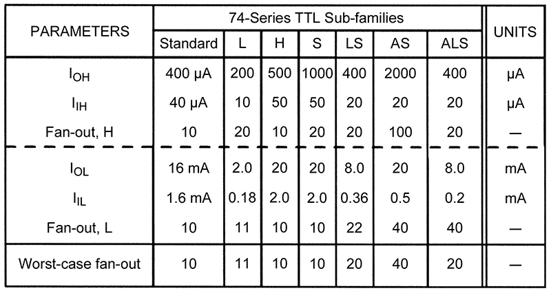
FIGURE 18. Fan-in and fan-out values of the major TTL sub-families.
When working within any one sub-family, note that the most important figure here is the ‘worst case fan-out (F-O)’ value. Thus, if you are (for example) designing a system based entirely on LS ICs, you can confidently connect an ordinary output directly to as many as 20 normal inputs, without risk of a malfunction due to overloading (if you need to drive more than 20 inputs, you can do so via one or more high-fan-out buffers, etc.). Note that, within any given sub-family, all ordinary inputs are said (in TTL jargon) to have a fan-in of unity (1), but that in practice some MSI or LSI ICs (such as counters and registers, etc.) may have special inputs (such as Reset or Preset, etc.) with fan-in values of two or greater.
Sometimes, an engineer may have to mix TTL sub-families, usually so that an obsolete IC can be replaced by a readily-available modern plug-in close-equivalent. In such a case, it is necessary to relate the fan-out data of one sub-family to that of another, to check that the mix can be made without causing an input or output overload. One easy way of doing this is to simply transpose the data of Figure 18 into ‘Standard TTL’ fan-in units, as shown in Figure 19, to gain an approximate idea of the relative fan values of various sub-families. Thus, it can be seen at a glance that LS TTL has only half of the fan-in requirement of Standard TTL, but also has only half of its fan-out capability, etc.
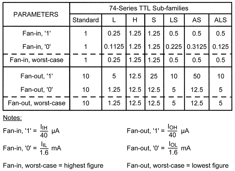
FIGURE 19. TTL fan-in and fan-out in terms of Standard TTL units.
An even more useful way of applying the basic data of Figure 18 is to convert it into an easily-used form that relates the fan-in and fan-out data of each TTL sub-family to all other TTL sub-families, as shown in Figure 20.
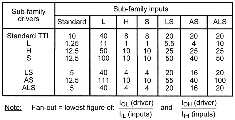
FIGURE 20. Maximum number of TTL inputs that may be driven from any TTL sub-family output.
Here, by reading across the left-hand columns, it can (for example) be seen that a normal LS output can drive up to five Standard TTL inputs, and that a Standard TTL output can safely drive up to 20 LS inputs.
Thus, if an engineer is faced with a problem such as that illustrated in Figure 21 — in which a fault on an old Standard TTL circuit is traced to a defective 74XXX-type IC (IC2) which is used to directly drive four other Standard TTL inputs — it can be quickly seen that a 74LSXXX plug-in equivalent IC can be safely used to directly replace the IC2 Standard TTL device without incurring overload problems.
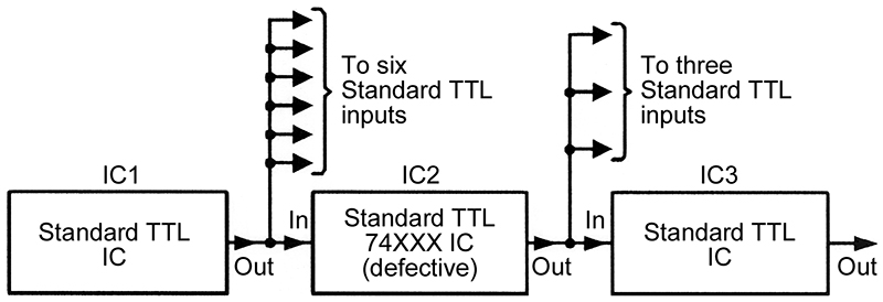
FIGURE 21. IC2 is defective; it is a Standard TTL device. Can it be replaced directly by a 74LSXXX IC? Figure 20 shows that the answer is yes.
TTL Basic Usage RulesIt is usually a fairly easy matter to design logic circuitry using TTL ICs, providing that a set of TTL basic usage rules are observed. Assuming that the matter of fan-in and fan-out has already been taken care of, there are four basic usage themes outstanding, and these will be described in our next installment, under the general headings of Power Supplies, Input Signals, Unused Inputs, and Interfacing. NV
The Wall